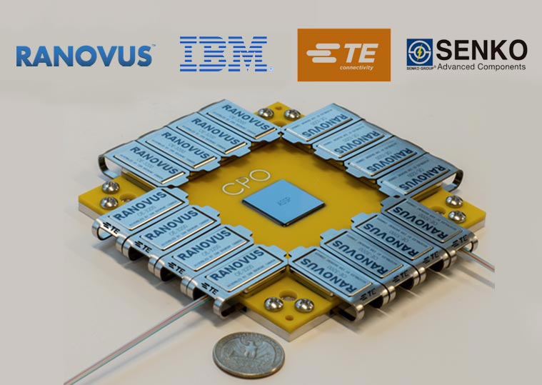
The Ranovus Odin™ 32 Co-Packaged Optics configuration for 51.2T Ethernet Switch application
Ranovus Odin™ 32 Co-Packaged Optics solution leverages this partnership
IBM will provide optical interconnect technologies that enable automated and scalable assembly for co-packaged optics
TE will demonstrate its CP fine pitch socket technology combined with thermal management using Thermal Bridge technology to illustrate integrated co-packaging solutions
SENKO will demonstrate its fiber optic connectivity solutions for optical coupling, on-board/mid-board, and faceplate
San Diego – March 12, 2020
Ranovus Inc. (“RANOVUS”) today announced a strategic collaboration with IBM Inc. (“IBM”), TE Connectivity (“TE”) and Senko Advanced Components, Inc (“SENKO”), leading providers of multi-terabit interconnect solutions, to create an ecosystem to design and manufacture multi-vendor solutions for Co-Packaged Optics applications in data center.
The collaboration leverages:
1- RANOVUS’ highly scalable Odin™ silicon photonics engine announced earlier (https://ranovus.com/ranovus-launches-its-single-chip-odin-silicon-photonic-engine-to-support-ml-ai-workloads-for-data-center-and-5g-mobility/). Odin™ incorporates the company’s disruptive innovation in multi-wavelength Quantum Dot Laser (QDL), 100Gbps Silicon Photonics based Micro Ring Resonator modulators and photodetectors, 100Gbps Driver, 100Gbps TIA and control Integrated Circuits in a power efficient and cost-effective EPIC in a single chip.
2- IBM’s innovative fiber V-groove interconnect packaging technology is a robust and reliable assembly technique to interface optical fibers to silicon photonics devices. This process makes use of passive alignment techniques and achieves low insertion loss across a wide spectral range in both the O-band and C-band regimes. The solution is scalable in physical channel count and the automated process provides a path to high-volume manufacturing of co-packaged optics.
3- TE’s co-packaged (CP) fine pitch socket interposer technology enables integration of small chipset and optical engine component technologies into high-value co-package assemblies with reworkable and interoperable interfaces. The signal integrity performance of the CP fine pitch socket interposer technology can be critical to 100 Gbps high density electrical packaging The integration of TE’s thermal bridge technology completes the assembly by providing an innovative solution for thermal management of the switch, serializer/deserializer (SerDes), and optics necessary for high reliability and long operating life.
4- SENKO’s fiber optic connectivity solutions for optical coupling, on-board/mid-board, and faceplate to support 100Gbps/lane and beyond Co-Packaged Optics equipment designs. These include low profile and precision Fiber coupler assemblies, micro sized on-/mid-board connectors, reflow compatible connector assemblies, and space saving connector options for faceplate. These will provide more efficiency, scalability, and flexibility in designs for Co-Packaged Optics equipment.
With data center traffic growing at an unprecedented pace, the networking infrastructure needs to scale in capacity while maintaining its total power consumption and footprint. Today’s disaggregated Ethernet switch IC and optical module architecture does not provide the scalability required to support the future growth of the data centers. Co-packaging of optics and Ethernet switch ICs is a natural next step to reduce the power consumption burden of the electrical I/Os in the data center networking equipment. The transition of the Ethernet switch IC SER/DES from 50Gbps to 100Gbps, in 25.6Tbps and 51.2Tbps switch configurations, presents a unique inflection point in the architecture of the Ethernet switch systems.
“RANOVUS’ Odin™ platform was conceived with miniaturized components such as Micro Ring Resonators in a monolithic Electronic and Photonic Integrated Circuit to deliver highly scalable solutions in support of single and multi-wavelength applications.” Said Georg Roell, Chief Technology Officer at Ranovus. “We are delighted to contribute our IP and create an ecosystem to remove a major hurdle for the adoption of Co-Packaged Optics solutions for data centers”.
“IBM is enthusiastic to bring to this collaboration more than 45 years history in microelectronics packaging and its deep experience in optical packaging,” said Paul Fortier, senior engineer, IBM business development. “IBM’s optical assembly processes leverage our automated high-volume semiconductor packaging and IBM’s Assembly and Test division provides the co-packaged optics ecosystem with a seamless end to end manufacturing capability.”
“TE is pleased to be able to bring decades of socket expertise to this co-packaging effort in the form of the fine pitch CP socket technology” said Nathan Tracy, Technologist, TE Connectivity, “In addition, TE’s thermal bridge technology is a key enabler to the high density packaging and extreme thermal management necessary for co-packaging”.
“SENKO is pleased to contribute our product designs, and IPs to enhance the design capability, scalability, and flexibility for the Co-Packaged Optics embedded products.” Said Tiger Ninomiya, Business Development / Product Line Manager at SENKO. “Innovative optical connectivity solutions are key to making Co-Packaged Optics’ solutions a success in the market.”
About Ranovus
Ranovus, with operations in Ottawa, Canada, Nuremberg, Germany and Sunnyvale, USA, develops and manufactures advanced solutions for the next generation of interconnects for the telecommunications and information technology industries. Our team has extensive experience in product development and commercialization of optoelectronics components and transceiver subsystems for the information technology industry. Ranovus’ current disruptive portfolio includes Quantum Dot Multi-Wavelength Laser technology and advanced digital and silicon photonics integrated circuit technologies that sets a new industry benchmark for the lowest power dissipation, size and cost for the next generation of optical interconnect solutions.
The company was founded in February 2012 and has received financing from leading venture capital firms including Azure Capital Partners, Deutsche Telekom Venture Funds, BDC Capital, OMERS Ventures, Export Development Canada, MaRS Investment Accelerator Fund, as well as Sustainable Development Technology Canada, and Strategic Innovation Fund of Canada. Additional information about Ranovus can be found at www.ranovus.com.
For more information, please contact:
Mike Newsom
LouVan Comm Inc.
+1-617-803-5385
mike@louvanpr.com
About IBM Canada
IBM Canada is headquartered in Markham, Ontario and is one of Canada’s top ten private R&D investors; contributing more than $478 million to Canadian research and development initiatives in 2017. IBM has a unique approach to collaboration that provides academic researchers, small and large business, start-ups and developers with business strategies and computing tools they need to innovate. Areas of focus include AI, cloud and security. Canada is also home to IBM’s largest microelectronics packaging and test facility in Bromont, Quebec and the largest software development organization in the country, with sites in Markham, Ottawa, and Fredericton.
For more information, please contact:
ibm.com/assembly
About TE
TE Connectivity is a $13 billion global industrial technology leader creating a safer, sustainable, productive, and connected future. Our broad range of connectivity and sensor solutions, proven in the harshest environments, enable advancements in transportation, industrial applications, medical technology, energy, data communications, and the home. With nearly 80,000 employees, including more than 8,000 engineers, working alongside customers in approximately 150 countries, TE ensures that EVERY CONNECTION COUNTS. Learn more at www.te.com and on LinkedIn, Facebook, WeChat and Twitter.
TE Connectivity, TE, TE connectivity (logo), and EVERY CONNECTION COUNTS are trademarks owned or licensed by the TE Connectivity Ltd. family of companies. Other logos, product(s) and/or company names might be trademarks of their respective owners.
Media Relations Contact:
Laetitia Donovan
TE Connectivity
(717) 986-7326
Laetitia.donovan@te.com
About SENKO
Senko Advanced Components is a wholly owned subsidiary of the SENKO Group, which is headquartered in Yokkaichi, Japan. From its humble beginnings in 1946. SENKO Advanced Components itself has 16 offices globally and dozens of design and manufacturing facilities providing local support to customers all around the globe. SENKO Advanced Components was incorporated in the United States in the early nineties and has since being recognized as one of the industry’s specialists in passive fiber optics interconnect and optical components. This is due in great part to the design capabilities and high manufacturing capacity in CNC machining, injection molding, and component assembly. To date, SENKO has over 100 awarded patents, with more than 140 pending.
SENKO Advanced Components develops, manufactures, markets and distributes over 1000 fiber optic products for the telecom & datacom industries worldwide. An ISO-9001 approved company, SENKO is able to provide multinational corporations with the technical expertise to liaise with engineers, and the manufacturing flexibility to develop custom products for the ever-growing high-tech industry. Many of our products were created to resolve a specific design challenge faced by our customers. We offer one of the industry’s largest product portfolios, and our quality is second to none. More information about SENKO can be found at www.senko.com.