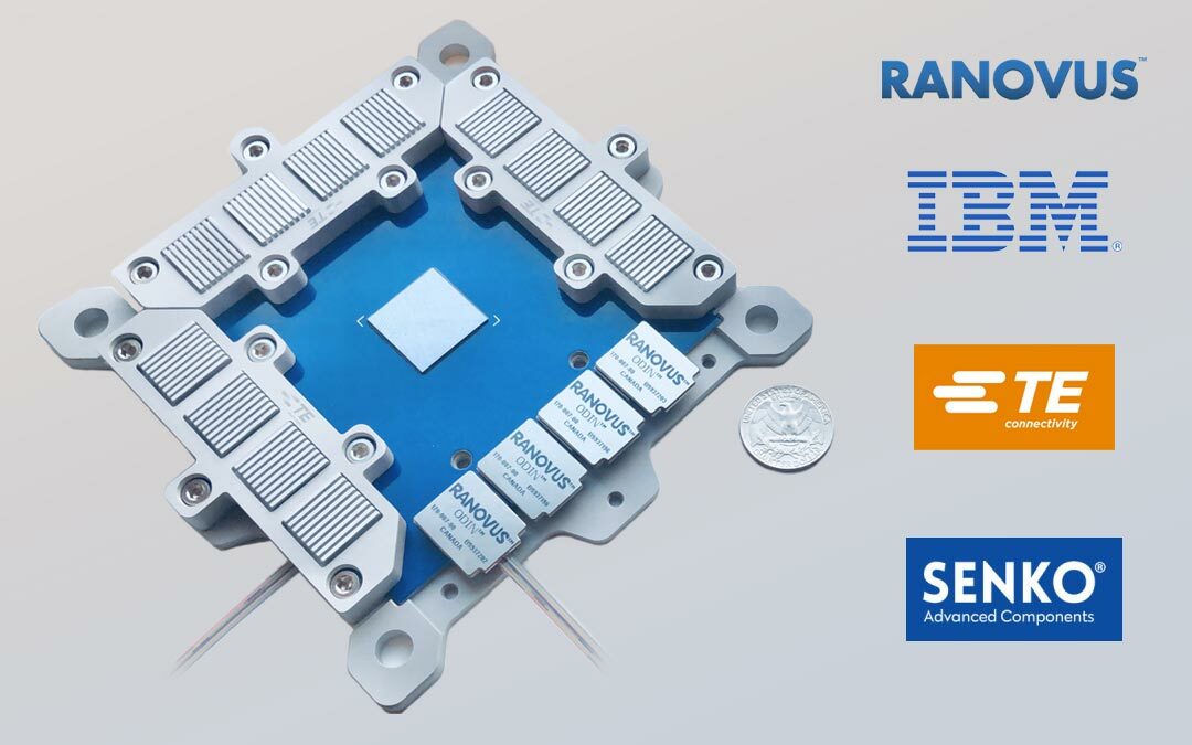
The Ranovus Odin™ Analog-Drive CPO 2.0 configuration for Ethernet Switch and ML/AI applications
Ranovus extends its partnership with IBM, TE Connectivity, and Senko Advanced Components to deliver significant power and cost savings with its “CPO 2.0” technology
San Francisco – June 7, 2021
Ranovus Inc. (“RANOVUS”) today announced at OFC 2021, the leading optical networking event in North America, the next step in reducing power consumption and overall costs for hyperscale data center operations with the introduction of the Odin™ Analog-Drive CPO 2.0 architecture. Ranovus has leveraged its strategic collaboration with IBM Inc. (“IBM”), TE Connectivity (“TE”), and Senko Advanced Components, Inc (“SENKO”), leading providers of multi-terabit interconnect solutions, to create a second[1]generation CPO 2.0 configuration for the data center. Co-packaged Optics, or CPO, is an innovative approach that provides nx100Gbps PAM4 Optical I/O for Ethernet switch and ML/AI silicon in a single packaged assembly, which significantly reduces the cost and power consumption of the complete system.
With data center traffic growing at an unprecedented pace, fueled by advances in AI and Machine Learning, the networking infrastructure must scale in capacity while maintaining its total power consumption and footprint. The strategic collaboration that was announced in March 2020 between 2 Ranovus, TE, IBM, and SENKO, known as CPO 1.0, has enabled an attractive multi-sourced solution to further meet this challenge.
CPO 2.0 improves on CPO 1.0 while maintaining optical interoperability and brings the following advantages to the ecosystem:
1- 40% cost and power consumption savings through: a. Eliminating the retimer function in the Odin™ Analog-Drive optical engine b. Enabling a cost-effective single die solution with the Odin™ Analog-Drive optical engine
2- Smaller footprint 3- Reuse and Optimization of existing 100G PAM4 and PCIe Ser/Des chips vs new investment in an XSR Ser/Des chip for data center applications Customer trials with Odin™ Analog-Drive CPO 2.0 are planned in Q4 2021. Specifically, this collaboration leverages
3- Reuse and Optimization of existing 100G PAM4 and PCIe Ser/Des chips vs new investment in an XSR Ser/Des chip for data center applications
Customer trials with Odin™ Analog-Drive CPO 2.0 are planned in Q4 2021
Specifically, this collaboration leverages:
1- RANOVUS’ highly scalable Odin™ silicon photonics engine announced at OFC 2020. Odin™ leverages the company’s disruptive innovation in Multi-Wavelength Quantum Dot Laser (MW QDL), 100Gbps Silicon Photonics based Micro Ring Resonator modulators and photodetectors, 100Gbps Driver, 100Gbps TIA and control circuity in a power efficient and cost-effective single die EPIC (Electronic-Photonic Integrated Circuit).
2- IBM’s innovative fiber V-groove interconnect packaging technology is a robust and reliable assembly technique to interface optical fibers to silicon photonics devices. This process makes use of passive alignment techniques and achieves low insertion loss across a wide spectral range in both the O-band and C-band regimes. The solution is scalable in physical channel count and the automated process provides a path to high-volume manufacturing of co-packaged optics.
3- TE Connectivity’s (TE) co-packaged (CP) fine pitch socket interposer technology enables integration of small chipset and optical engine component technologies into high-value co[1]package assemblies with reworkable and interoperable interfaces. The CP fine pitch socket interposer technology has signal integrity performance capability for 100 Gbps as well as future 200 Gbps applications. The integration of TE’s controlled force mechanical and thermal bridge hardware completes the assembly by providing an innovative solution for thermal management of the switch, serializer/deserializer (SerDes), and optics necessary for high reliability and long operating life.
4- SENKO’s fiber optic connectivity solutions for optical coupling, on-board/mid-board, and faceplate support 100Gbps/lane and beyond Co-Packaged Optics equipment designs. These include low profile and precision fiber coupler assemblies, micro sized on-/mid-board connectors, reflow compatible connector assemblies, space saving connector options for faceplate, and blindmate connector solutions for backplane and external laser source modules. These will provide more efficiency, scalability, and flexibility in designs for Co-Packaged Optics equipment.
“We launched Odin™, our next generation monolithic EPIC and laser platform for multi terabit Co[1]Packaged Optics (CPO) applications in data centers, in March 2020. The Odin™ platform is a low latency, high density, protocol agnostic monolithic optical engine that delivers massive optical interconnect bandwidth with industry-leading cost and power efficiency,” said Dr. Christoph Schulien, EVP of R&D and Systems at Ranovus. “The Odin™ Analog-Drive configuration eliminates the retimers in the CPO 1.0 configuration, which brings about a 40% cost and power reduction to the overall system.”
IBM is enthusiastic to bring to this collaboration more than 45 years history in microelectronics packaging and its deep experience in optical packaging,” said Paul Fortier, senior engineer, IBM business development. “IBM’s optical assembly processes leverage our automated high-volume semiconductor packaging and IBM’s Assembly and Test division provides the co-packaged optics ecosystem with a seamless end to end manufacturing capability.”
“TE is bringing a holistic solution set to the Co-Packaging effort with our electrical interconnect CP socket technology that can enable CPO miniaturization along with reworkability,” said Nathan Tracy, Technologist, TE Connectivity, “TE’s thermal bridge technology can be a key enabler to the high density packaging and extreme thermal management necessary for co-packaging.”
“SENKO is pleased to contribute our product designs, and IPs to enhance the design capability, scalability, and flexibility for the Co-Packaged Optics embedded products.” Said Tiger Ninomiya, (Technology & Innovation Manager) at SENKO. “Innovative optical connectivity solutions are key to making Co-Packaged Optics’ solutions a success in the market.”
About Ranovus
Ranovus, with operations in Ottawa, Canada, Nuremberg, Germany and Sunnyvale, USA, develops and manufactures advanced photonics interconnect solutions to support the next generation of AI/ML workloads in data centers and communication networks. Our team has extensive experience in product development and commercialization of optoelectronics subsystems for the information technology industry. Ranovus’ current disruptive portfolio includes Multi-Wavelength Quantum Dot Laser technology and advanced digital and silicon photonics integrated circuit technologies that set a new industry benchmark for the lowest power dissipation, size, and cost for the next generation of optical interconnect solutions. Ranovus’ Odin™ platform is the enabling technology for a new data center architecture optimized for AI/ML workloads.
Information about Ranovus can be found at www.ranovus.com.
For more information, please contact:
Mike Newsom
LouVan Comm Inc.
+1-617-803-5385
mike@louvanpr.com
About IBM Canada
IBM Canada is headquartered in Markham, Ontario and is one of Canada’s top ten private R&D investors; contributing more than $478 million to Canadian research and development initiatives in 2017. IBM has a unique approach to collaboration that provides academic researchers, small and large business, start-ups and developers with business strategies and computing tools they need to innovate. Areas of focus include AI, cloud and security. Canada is also home to IBM’s largest microelectronics packaging and test facility in Bromont, Quebec and the largest software development organization in the country, with sites in Markham, Ottawa, and Fredericton.
IBM and the IBM logo are trademarks of International Business Machines Corp., registered in many jurisdictions worldwide. Other product and service names might be trademarks of IBM or other companies. A current list of IBM trademarks is available on the Web: Copyright and trademark information. www.ibm.com/legal/copytrade.shtml
For more information, please contact:
ibm.com/assembly
About TE
TE Connectivity is a $12 billion global industrial technology leader creating a safer, sustainable, productive and connected future. Our broad range of connectivity and sensor solutions, proven in the harshest environments, enable advancements in transportation, industrial applications, medical technology, energy, data communications and the home. With approximately 80,000 employees, including more than 7,500 engineers, working alongside customers in approximately 140 countries, TE ensures that EVERY CONNECTION COUNTS. Learn more at www.te.com and on LinkedIn, Facebook, WeChat and Twitter.
TE Connectivity, TE, TE connectivity (logo), and EVERY CONNECTION COUNTS are trademarks owned or licensed by the TE Connectivity Ltd. family of companies. Other logos, product(s) and/or company names might be trademarks of their respective owners.
Media Relations Contact:
Bianca Koop
TE Connectivity
(519) 319 2448
Bianca.koop@te.com
About SENKO
Senko Advanced Components is a wholly owned subsidiary of the SENKO Advance, which is
headquartered in Yokkaichi, Japan. With16 locations globally, and dozens of design and manufacturing
facilities providing local support to customers all around the globe. SENKO was incorporated in the United
States in the early nineties and has since being recognized as one of the industry’s specialists in passive
fiber optics interconnect and optical components. This is due in great part to full vertical integration from
the design capabilities, qualification/testing, and manufacturing. SENKO has deployed over 700 million
connectors. To date, SENKO has over 150 awarded patents, with more than 300 pending.
SENKO develops, manufactures, markets and distributes over 1000 fiber optic products for the telecom &
datacom industries worldwide. An ISO-9001 approved company, SENKO is able to provide multinational
corporations with the technical expertise to liaise with engineers, and the manufacturing flexibility to develop
custom products for the ever-growing high-tech industry. Many of our products were created to resolve a
specific design challenge faced by our customers. We offer one of the industry’s largest product portfolios,
and our quality is second to none. More information about SENKO can be found at www.senko.com